
In the realm of modern electronic equipment, the solder ball grid array (BGA soldering) stands out as a powerhouse, offering small and exquisite packages with robust functionality. This article will guide you through the intricacies of BGA soldering, unlocking the potential of compact yet powerful electronic devices.
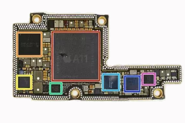
BGA packaging revolutionizes chip design by featuring a dot matrix of pads on the chip's bottom, connected to the PCB board through uniform solder balls. Compared to traditional packaging with lead pins, BGA significantly increases pin count and enhances heat dissipation, presenting both advantages and challenges for board repair.
Disassembling and reinstalling a BGA chip poses unique challenges. The delicate solder balls at the bottom can be easily damaged during disassembly. Special tools are required for desoldering, and precise steel meshes, often laser engraved, are essential for realigning solder balls with the chip's pads.
Now, let's delve into the comprehensive 18-step manual for replanting solder balls and the soldering process:
Apply a supporting steel mesh on the chip's bottom pins, evenly spreading solder paste and pressing firmly.
Clean remaining solder paste with a soft cloth, ensuring uniform distribution on all pins.
Use pointed tweezers to remove solder paste from the top four core alignment pads.
Heat the stencil and chip with a hot air gun until solder paste melts and forms balls.
Apply Solder Pastes Flux, heat again for uniform solder ball formation.
Separate the stencil using pointed tweezers, then use a tin-absorbing copper screen to remove excess solder.
After cooling, clean the chip's surface with a cleaning solution and a soft cloth.
Use a fine needle to remove fibers left on the chip's surface during cleaning.
Remove impurities around the chip's edge with a carving knife.
Carefully observe and repair any defects in solder balls, testing patience and eyesight.
Add solder paste to defective solder balls and reheat with a hot air gun.
Use a thin needle to disconnect tin bridges formed during reheating.
Clean the PCB pad surface with a knife-edge soldering iron before placing the chip.
Heat the chip evenly with a hot air gun until solder pads melt and fuse with the PCB.
Gently touch the chip's edge with a thin needle to ensure automatic alignment.
Infiltrate the chip's bottom with flux, continue heating with a hot air gun.
Observe the chip's alignment and neatness as flux increases fluidity.
Once cooled, visually confirm successful soldering of all chip pins to the bottom PCB.
Understanding the intricacies of BGA soldering involves the collaborative efforts of solder, pad, heat, and flux. While not every electronic engineer may use a magnifying microscope, a single observation of the soldering process outlined above can leave a lasting impression, subtly influencing your operations in future soldering endeavors.
Reading more>>>>>
 WhatsApp